
Engineering a more accessible future for ultrafast lasers.
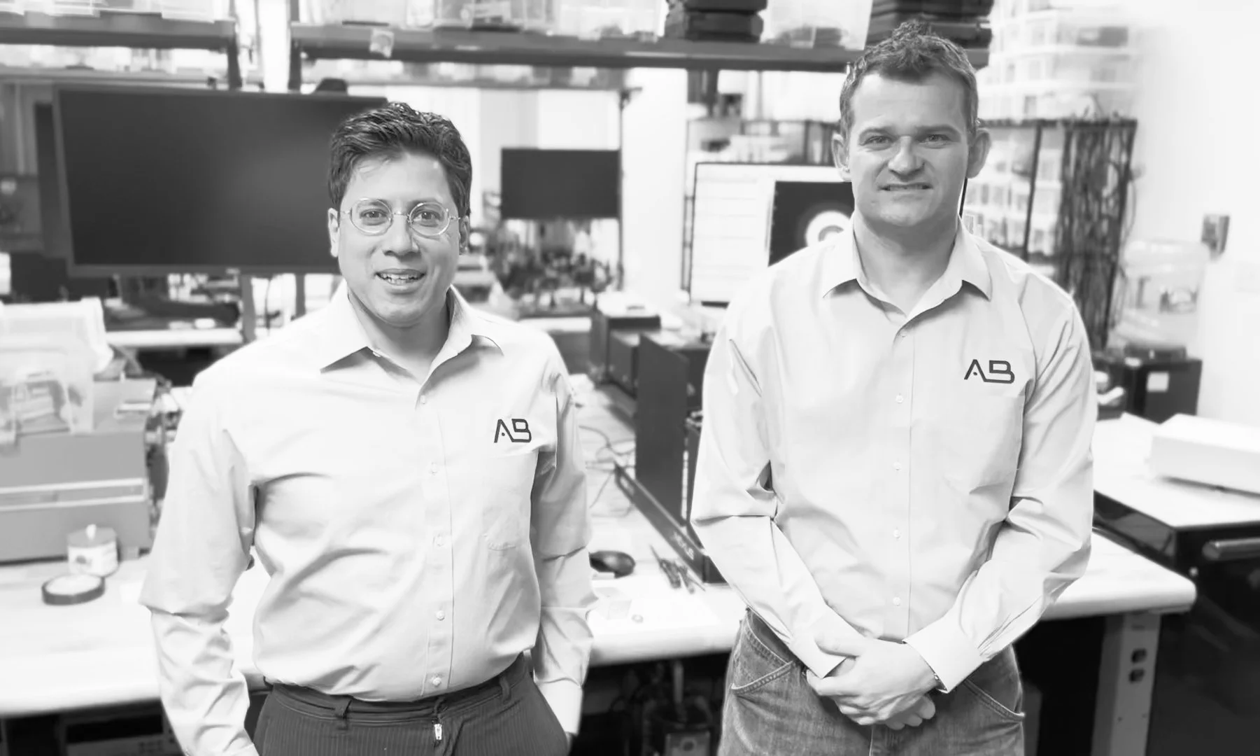
Built by people who have taken optical systems from first prototype to production.

ABOUT AB PHOTONICS
AB Photonics was founded in March 2023 by engineers with decades of experience developing lasers, optical instruments, and manufacturing systems.
Throughout their careers, they saw the same problem repeatedly: promising instruments constrained by laser sources that were too large, too costly, or too difficult to scale.
AB Photonics was created to approach that problem differently.
Make ultrafast lasers accessible to more customers and more applications.
That mission guides what we design, how we manufacture, and how we work with customers.
We want more teams to move advanced techniques beyond specialized research environments and into instruments that can reach new markets, expand scientific capabilities, and create meaningful customer value.
OUR MISSION
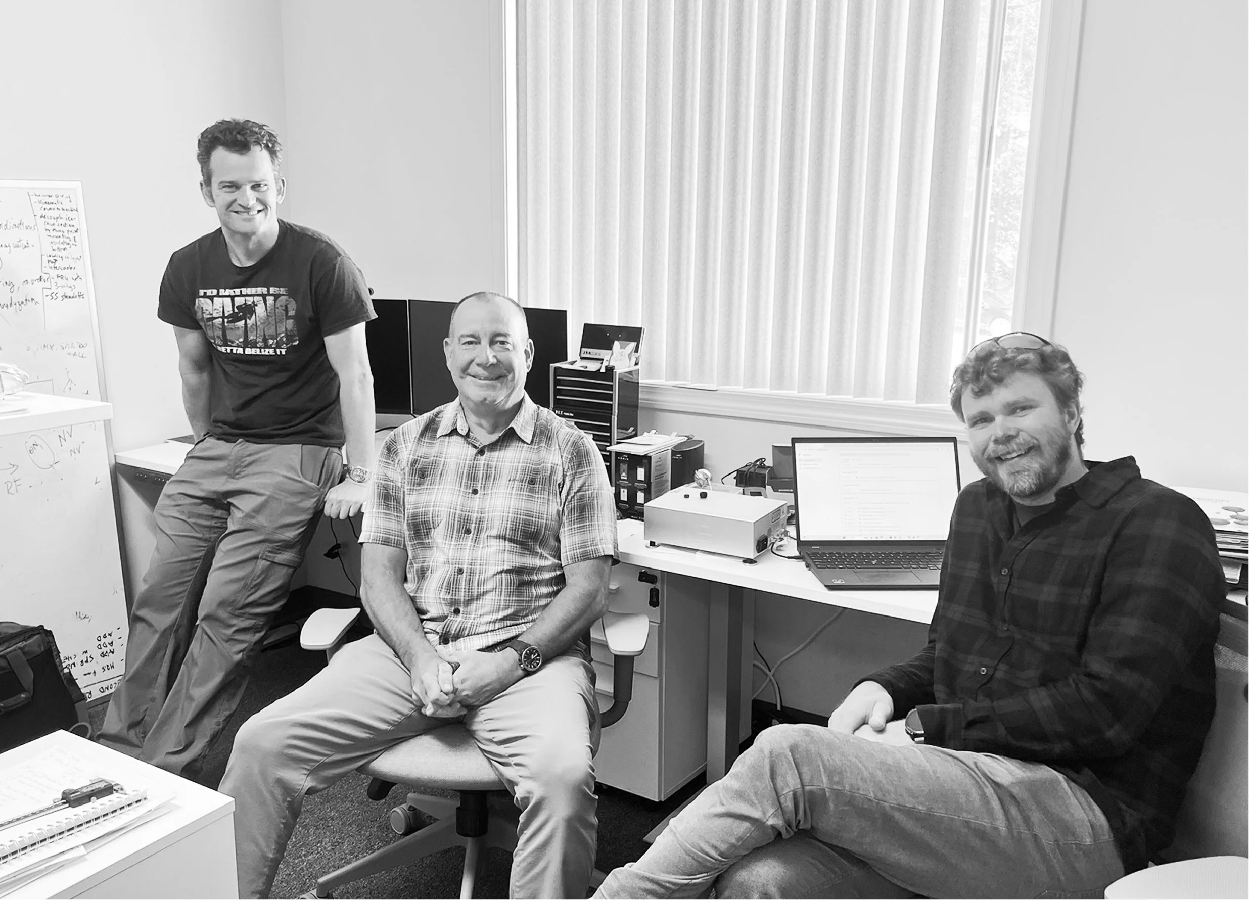
Start With the Application
We begin by understanding what the instrument needs to accomplish. That includes its performance requirements, physical constraints, development stage, and path toward production.
How We Work
Consider Production From the Beginning
Manufacturing and scalability are part of the design process, not problems left for later. Our systems are developed with repeatable assembly, testing, and commercial volume in mind.
Keep Engineers Close to the Customer
Customers work directly with the people designing and building the laser. Feedback moves quickly, technical questions reach the right person, and the system can evolve around real product requirements.
CONNECTICUT OPERATIONS
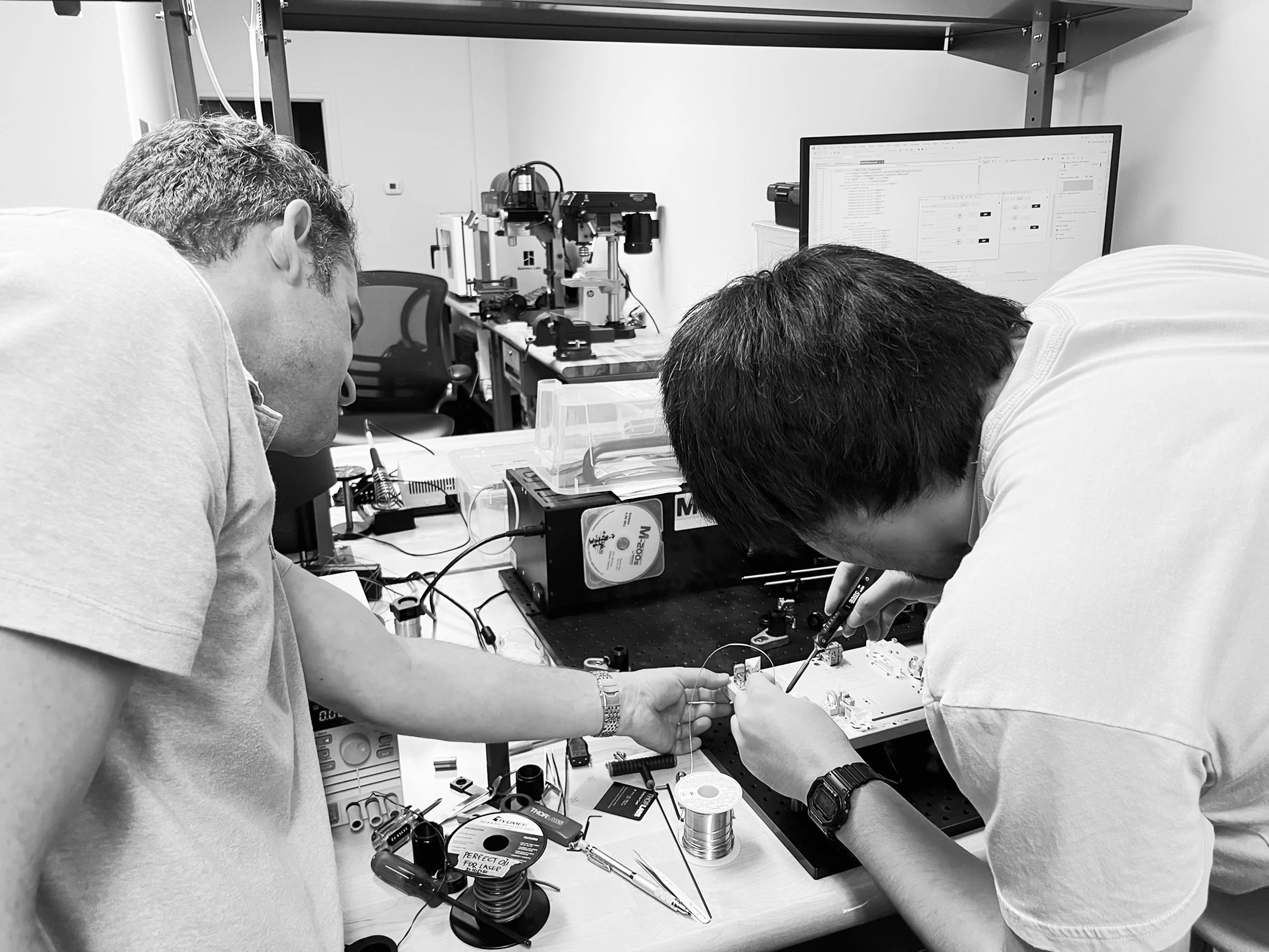
Designed, built, and tested in Guilford, Connecticut.
AB Photonics designs, manufactures, assembles, and tests its lasers at our facility in Guilford.
Keeping these capabilities together gives our team direct visibility into quality, manufacturing, supply, and every system we ship. It also keeps customer feedback close to the engineers who can act on it.
Founded in 2023
Guilford, Connecticut
U.S.-based engineering and manufacturing
Direct customer support
Leadership
Experience across the lab, factory, and product roadmap.
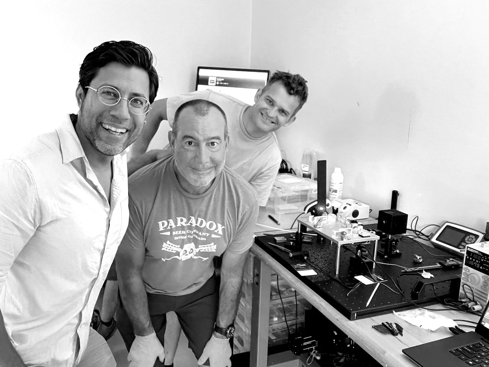
The AB Photonics co-founders combine academic depth with industry experience in laser physics, optoelectronics, microscopy, semiconductor devices, biotech instrumentation, optical metrology, and manufacturing.
Faisal Ahmad, PhD
Co-Founder & CEO
Faisal is a physicist and technology leader with more than two decades of experience in semiconductor devices, optoelectronics, laser systems, and advanced optical instrumentation. His work has spanned early research, prototype development, manufacturing systems, and the commercialization of complex scientific technologies.
Pat Adcock
President & COO
Pat is an operations and manufacturing leader with more than 35 years of experience guiding technology companies from startup through commercial growth. His background spans biotech, energy storage, and advanced manufacturing, with expertise in supply chain, new product introduction, and scaled production. He brings the operational experience needed to move innovative systems into reliable, repeatable manufacturing.
Michael Bellos, PhD
Co-Founder & CTO
Michael is an optical engineer and physicist specializing in laser technology, microscopy, and optical system development. His experience includes commercial laser development, advanced biotech instrumentation, manufacturing scale-up, system reliability, and the transition of complex technologies into practical products.

Tell us what you want to make possible.
Whether you are refining an existing instrument, exploring a new application, or preparing a platform for production, our engineering team is ready to listen.